- 810 Lawrence Drive, Unit 102 Thousand Oaks, CA 91320
- 1-(805)-581-6800
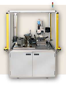
NIR Automatic Inspection Microscope
Details
The McBain NIR 200 is a fully-automated near-infrared inspection system for extracting wafers from a source cassette and measuring multiple alignment targets with 0.5 micron repeatability. The tool can be run in manual, local auto or full remote through GEM/SECS.


NIR Automatic Inspection Microscope
Features:
- Automatic loading and unloading of 4″, 6″ and 8″ wafers
- Motorized X, Y, Z and theta axis
- 900nm to 1700nm custom optical system provides best-in-class NIR visibility
- Highly sensitive InGaAs camera
- Integrated vision system and customizable software for:
- Image optimization
- Part recipe
- Palletization
- Critical measurements
- Defect detection and classification
- 6 inches of vertical Z travel allows custom tooling
- 6″, 8″ or 12″ travel XY stage options
- solid reflected or transmitted light
- manual coarse, fine or motorized options
- 0.5 micron feature resolution
- 0.1 micron positioning accuracy and repeatability
- Turnkey integrated motion control packages
- Ergonomic 3 axis joystick and trackball controls
- Vibration isolation
- Custom configurations available
Fully-automatic Measuring and Alignment Microscope and Handling System
The McBain NIR 200 is a fully-automated near-infrared inspection system for extracting wafers from a source cassette and measuring multiple alignment targets with 0.5 micron repeatability. The tool can be run in manual, local auto or full remote through GEM/SECS.
The NIR200 is a reliable production tool that is highly configurable to end-user needs. Throughput is partly dependent on the number of sites per wafer; a nine-site inspection set-up can run a cassette of 25 wafers in 45 minutes. The NIR200 is best-in-class for wafer-to-wafer and die-to-die critical alignment measurement and verification. This unique tool has been sold into many industries and a range of applications including sub-surface wafer and die inspection for cracks and bond integrity, MEMS, wafer bonding, 3-D chip stacking, failure analysis, process development, tool verification, part characterization, environmental testing and more.
See also the semi-automatic version of this tool.
We can ship this item worldwide. If you would like a specific quote and estimated delivery time, contact us today.
