Smaller, faster, cheaper – it’s the mantra of microelectronics. Moore’s Law in action. With electronic devices getting smaller and more complex the problem of inspection during the manufacturing process to ensure the product is fault free is also complex.
Each new generation of product must outperform its predecessors, in smaller package sizes and without significant increases in costs. As the size of electronic devices continues to get smaller, the need for increasingly powerful measurement techniques becomes even more important. At smaller scales, the effect of every imperfection becomes magnified, while new design complications begin to have a measurable impact on performance. Investments in high-performance microscope systems can ensure microelectronics inspection is performed with a high degree of quality and repeatability.
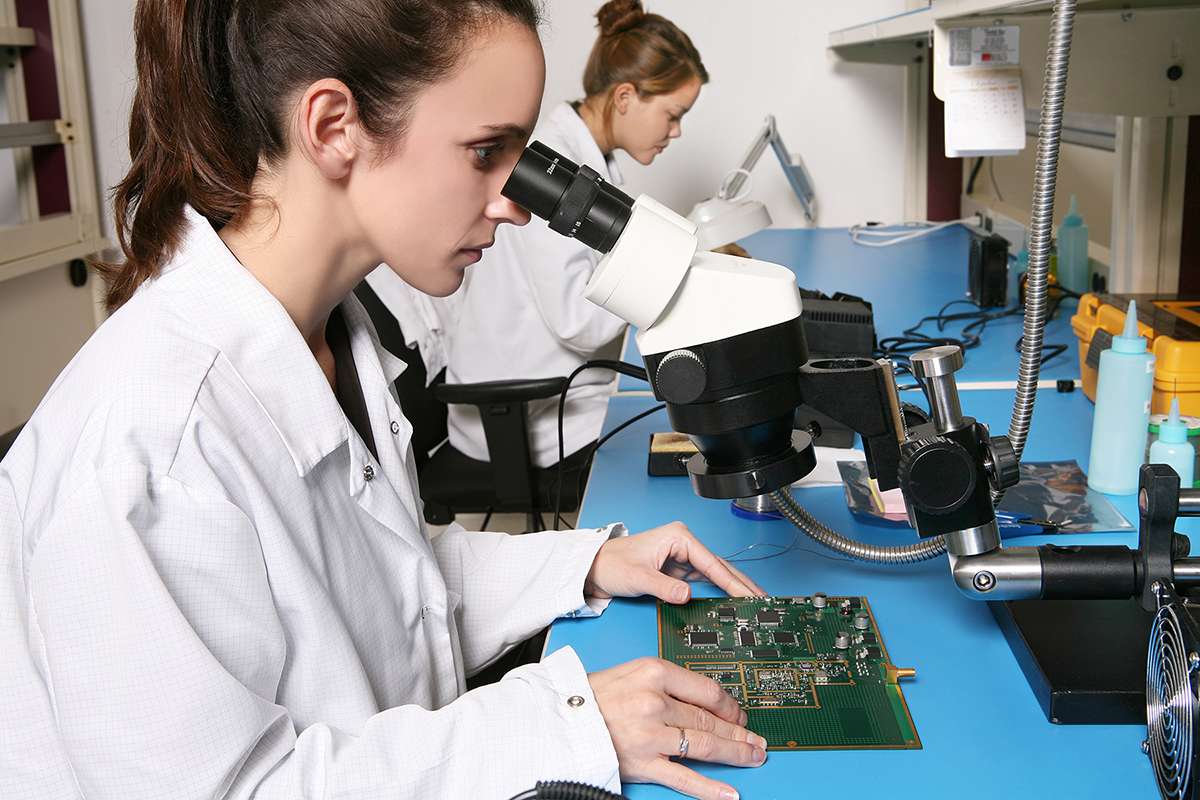
For over a decade McBain has been supporting factories in Silicon Valley and around the world with a portfolio of innovative, cost-efficient and highly effective solutions for microelectronics inspection. McBain’s tools often replace outdated inspection methods, ineffective equipment, or even more expensive semiconductor inspection systems that fail to address specific needs. McBain’s solutions may fit your needs more elegantly, more simply, and at lower cost.
McBain’s systems address such applications as wafer defect inspection, infrared inspection, macro and micro inspection, probe card inspection, small field mask aligning, laser autofocusing, wafer handling and a lot more.
Unlike the large equipment makers, McBain is ready, willing and fully able to modify, customize and even develop whole new systems precisely for your specific needs. Contact McBain Systems today for a free consultation.