- 810 Lawrence Drive, Unit 102 Thousand Oaks, CA 91320
- 1-(805)-581-6800
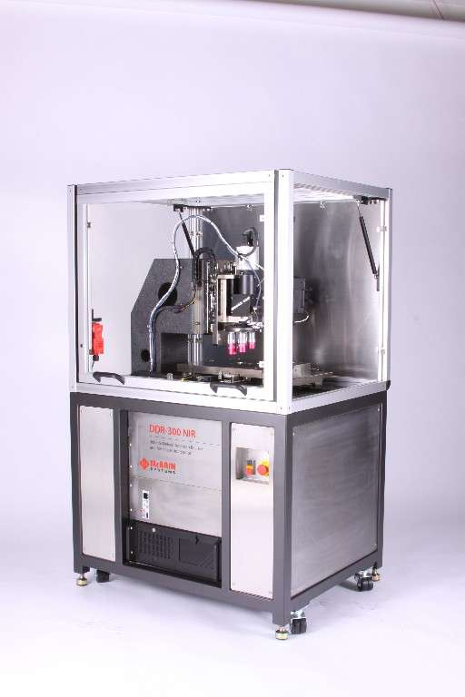
McBain DDR200/300 NIR-SWIR Infrared Microscope
Details
The McBain DDR200 NIR (for 200mm) and DDR300 NIR (for 300mm) provide high-speed defect detection and precision measurement on wafers and other parts. These cost-efficient systems offer unique advantages for both production and process development use, providing an optimum near-infrared (900-1700nm) solution when both subsurface defect detection and dimensional metrology are required.
McBain DDR200/300 NIR-SWIR Infrared Microscope
Features:
- Designed for automatic / semiautomatic operation
- Extensive defect detection features and capability
- Integrated dimensional metrology features
- Able to penetrate thicker materials, more highly doped materials and rougher surfaces than other systems
- Submicron-precision optical measurements
- High-accuracy staging, to 20nm linear encoder resolution
- Highest resolution 900-1700nm InGaAs digital camera in class
- High-speed linear servo motor staging
- 50-500 defects/measurement/second per field of view, typical
- Very easy to use, program and set up
- Multiple wafer/die/part handling systems available
- Application-specific customizable software
- Semi Standard S2/S8 compliant
Near Infrared Subsurface Defect Detection and Review Systems
The McBain DDR200 NIR (for 200mm) and DDR300 NIR (for 300mm) provide high-speed defect detection and precision measurement on wafers and other parts. These cost-efficient systems offer unique advantages for both production and process development use, providing an optimum near-infrared (900-1700nm) solution when both subsurface defect detection and dimensional metrology are required.
These DDR systems feature a powerful set of automated and semi-automated optical and digital video tools, which are optimized for high accuracy, production throughput and ease of use. The automated and versatile platform features McBain’s state-of-the-art near-infrared Koehler Epi-illumination as well as optional transmitted-illumination packages. All systems are configured on McBain Systems’ precision multi-axis platforms.
Applications
- For in-process, post-process and failure analysis
- Bonded wafer alignment
- Die alignment (flip-chip or hybridization)
- Subsurface defect visualization, detection, characterization
- MEMS device inspection and metrology
- 3D stacking process development and control
We can ship this item worldwide. If you would like a specific quote and estimated delivery time, contact us today.